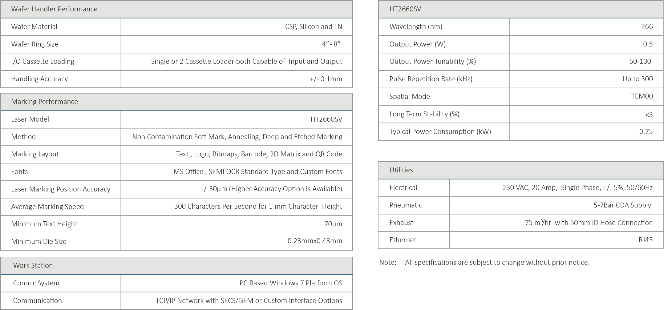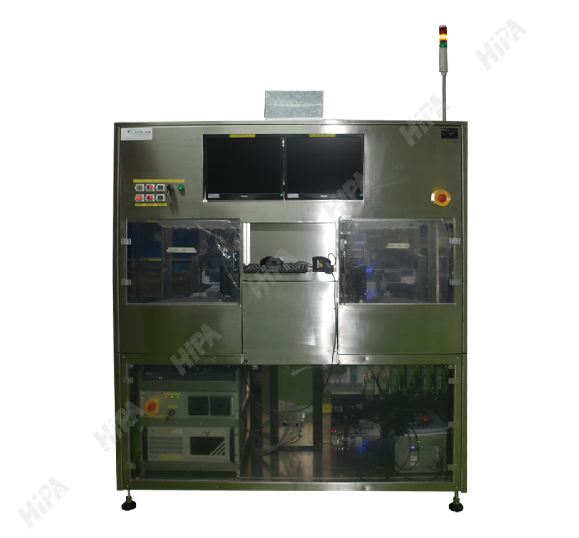
As the industry advances toward miniaturization and new materials composite on the wafer, the demand for wafer and individual die marking for traceability and identification has increased in the recent years. Capitalizing on our scanvision capability and laser knowledge, Hylax direct wafer die marking system is a fully automatic system designed for direct marking of dies in post sawn wafer form in wafer rings and capable of processing up to 12” wafer size.
如需中文资料请E-mail:james@hylax.com
Smart and accurate loading and unloading through robotic cassette scanning and wafer handling
Fast and accurate laser marking through scanvision pre-alignment image technique
Real time quality check method through incorporated post mark inspection
Best consistent quality marking through dynamic focus height compensation for warp wafers
Flexible marking layout and wafer mapping capability through data download from host link communication with SECS/GEM option
Windows based user friendly interface software provides flexibility and rapid model change
Low utility cost and maintenance-friendly design with intelligent diagnostic functions


